Hi, I have Nvidia Orin AGX.
I want to use GPIO9 (32 pin on 40 pin expansion header, mapped to 356 GPIO on system-PBB.00) and GPIO17 (22 pin on 40 pin expansion header, mapped to 444 GPIO on system-PP.04) inside my custom I2C driver.
Device tree overlay should go something like this:
/dts-v1/;
/plugin/;

/ {
    fragment@0 {
        target-path = "/bus@0/i2c@c250000";  // I2C SW bus 7, or pins 3 and 5 on 40 pin connector
        __overlay__ {
            #address-cells = <1>;
            #size-cells = <0>;
            mysensorxbg@69 {
                compatible = "mysensorxbg";
                reg = <0x69>;
                // Interrupt pin, GPIO17 as low
                sensor,int-gpios = <0xf1 0x1BC 0x00>;
                // Reset pin, GPIO9 as low
                sensor,resetn-gpios = <0xf1 0x164 0x00>;
                status = "okay";
            };
        };
    };
};
Where 0xf1 is phandle of gpio controller “2200000”.
After that I want to use this pin inside driver probe function like this:
  resetn_gpio = gpiod_get(&client->dev, "sensor,resetn", GPIOD_OUT_LOW);
  if (IS_ERR(resetn_gpio))
  {
      pr_err("%s: Failed to get RESETN GPIO pin from device tree!\n", __func__);
      return -EINVAL;
  }
But this fails with error mesage:
[   59.917908] mysensorxbg_probe triggered.
[   59.917956] mysensorxbg_probe: INT pin '-2081705472' successfully retrieved from device tree!
[   65.382240] mysensorxbg_remove triggered.


[   66.590710] mysensorxbg_probe triggered.
[   66.590736] mysensorxbg_probe: Failed to get INT GPIO pin from device tree!
[   66.590740] mysensorxbg: probe of 7-0069 failed with error -22
NOTE: Pins are unused when listed using “sudo /opt/nvidia/jetson-io/jetson-io.py”.
I am new to Orin device, so not sure if I am missing something.
Are you using the devkit or custom board for AGX Orin?
What’s the Jetpack version in use?
PP.04 is configured as TEGRA234_MAIN_GPIO(P, 4) in device tree source, which mapping to 0x74 so that you should configure it as following:
sensor,int-gpios = <0xf1 0x74 0x00>;
Please refer to tegra234-gpio.h for details.
You said that 0xf1 is the phandle of GPIO controller (2200000), but PBB.00 belongs to AON-GPIO controller(c2f0000) so that you have to use the phandle of AON-GPIO controller instead of 0xf1 here.
If I use define TEGRA234_MAIN_GPIO_PORT_P 14 + offset from device tree TEGRA234_MAIN_GPIO(P, 4) under gpio@2200000 it will be 0x74 or 116 in decimal.
Regarding PBB.00 (pin 32 on 40 pin header) I saw yesterday that it belongs to second gpiochip.
Anyways, I wrote this simple C program:
#include <stdio.h>
#include <gpiod.h>
#include <unistd.h>

#define GPIO_CHIP_NAME "/dev/gpiochip1" // GPIO chip device (c2f0000)
#define GPIO_LINE 8 //This is pin 32 on 40 pin header (PBB.00)

int main() {
    struct gpiod_chip *chip;
    struct gpiod_line *line;
    int ret;

    // Open the GPIO chip
    chip = gpiod_chip_open(GPIO_CHIP_NAME);
    if (!chip) {
        perror("Failed to open GPIO chip");
        return 1;
    }

    // Get the GPIO line
    line = gpiod_chip_get_line(chip, GPIO_LINE);
    if (!line) {
        perror("Failed to get GPIO line");
        gpiod_chip_close(chip);
        return 1;
    }

    // Request the GPIO line as an output
    ret = gpiod_line_request_output(line, "gpio_control", 0);
    if (ret < 0) {
        perror("Failed to request GPIO line as output");
        gpiod_chip_close(chip);
        return 1;
    }

    // Print line information
    unsigned int line_num = gpiod_line_offset(line);
    const char *line_name = gpiod_line_name(line);
    printf("Line information:\n");
    printf("Line number: %u\n", line_num);
    printf("Line name: %s\n", line_name ? line_name : "Unnamed");

    // Set the GPIO line value to low (0)
    ret = gpiod_line_set_value(line, 0);
    if (ret < 0) {
        perror("Failed to set GPIO line value to 0");
        gpiod_chip_close(chip);
        return 1;
    }

    // Read and print the state after setting to 0
    int value = gpiod_line_get_value(line);
    if (value >= 0) {
        printf("Line value after setting to 0: %d\n", value);
    } else {
        perror("Failed to read line value after setting to 0");
    }

    sleep(10);

    // Set the GPIO line value to high (1)
    ret = gpiod_line_set_value(line, 1);
    if (ret < 0) {
        perror("Failed to set GPIO line value to 1");
        gpiod_chip_close(chip);
        return 1;
    }

    // Read and print the state after setting to 1
    value = gpiod_line_get_value(line);
    if (value >= 0) {
        printf("Line value after setting to 1: %d\n", value);
    } else {
        perror("Failed to read line value after setting to 1");
    }

   sleep(10);

    // Release the GPIO line and close the chip
    gpiod_chip_close(chip);

    return 0;
}
Output of program is next:
Line information:
Line number: 8
Line name: PBB.00
Line value after setting to 0: 0
Line value after setting to 1: 1
gpioinfo output is next:
gpiochip1 - 32 lines:
        line   0:     "PAA.00"       unused   input  active-high
        line   1:     "PAA.01"       unused   input  active-high
        line   2:     "PAA.02"       unused   input  active-high
        line   3:     "PAA.03"       unused   input  active-high
        line   4:     "PAA.04"       unused   input  active-high
        line   5:     "PAA.05"       unused   input  active-high
        line   6:     "PAA.06"       unused   input  active-high
        line   7:     "PAA.07"       unused   input  active-high
        line   8:     "PBB.00" "gpio_control" output active-high [used]
        line   9:     "PBB.01"       unused   input  active-high
        line  10:     "PBB.02"       unused   input  active-high
        line  11:     "PBB.03"       unused  output  active-high
        line  12:     "PCC.00"       unused   input  active-high
        line  13:     "PCC.01"       unused   input  active-high
        line  14:     "PCC.02"       unused   input  active-high
        line  15:     "PCC.03"       unused   input  active-high
        line  16:     "PCC.04"       unused  output  active-high
        line  17:     "PCC.05"       unused   input  active-high
        line  18:     "PCC.06"       unused   input  active-high
        line  19:     "PCC.07"       unused   input  active-high
        line  20:     "PDD.00"       unused   input  active-high
        line  21:     "PDD.01"       unused   input  active-high
        line  22:     "PDD.02"       unused   input  active-high
        line  23:     "PEE.00"       unused   input  active-high
        line  24:     "PEE.01"       unused   input  active-high
        line  25:     "PEE.02"       unused   input  active-high
        line  26:     "PEE.03"       unused   input  active-high
        line  27:     "PEE.04"      "Power"   input   active-low [used]
        line  28:     "PEE.05"       unused   input  active-high
        line  29:     "PEE.06"       unused   input  active-high
        line  30:     "PEE.07"       unused   input  active-high
        line  31:     "PGG.00"       unused   input  active-high
I can see here that my program is controlling it, but the problem is that pin state does not change.
It is stuck to 3.3V when I connect multimeter to it, to pin 32 on 40 pin header. When code sets it to low state, voltage is still 3.3V.
Why is pin state not changing even tough software says it is?
Is this related to device tree configuration, because it is set to input pin:
Also PBB.00 is 324 using link from above, but if I calculate it using TEGRA234_AON_GPIO I will get:
1x8 + 0 = 8. So does this 8 represents number I should use for this pin in device tree like:
you cannot change the value of a gpio pin which is configured as “Input”.
You need to configure its direction as “Output” so that you can successfully toggle the values between 0 and 1.
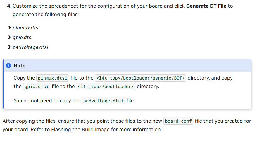
I am trying to find the steps to update pinmux configuration.
I found excel sheet “Orin_Jetson_Series_Pinmux_Config_Template_2.0.xlsm” that is used to generate new dtsi files, but how do I apply them to system?
There are no useful links for this…
When I was flashing Orin first time, I used next command:
sudo ./flash.sh jetson-agx-orin-devkit mmcblk0p1
This means flash script will use “jetson-agx-orin-devkit.conf” configuration file.
Picture from above states that once I generate pmux and gpio files, I should copy them to specified location then point to them inside new board conf file.
How do I add these new files to new board config file?
I tried to use “jetson-agx-orin-devkit.conf” to track things:
“jetson-agx-orin-devkit.conf” includes “p3737-0000-p3701-0000.conf.common” that includes “p3701.conf.common” that defines:
But this is dts file not dtsi file, so I do not understand how to add my newly generated files, where I changed pins from input to output and verified changes inside them.
So if I check tegra234-mb1-bct-pinmux-p3701-0000-a04.dtsi it includes tegra234-mb1-bct-gpio-p3701-0000-a04.dtsi file that contains GPIO definitions.
So I guess if I change tegra234-mb1-bct-pinmux-p3701-0000-a04.dtsi to pinmux.dtsi and also inside of pinmux.dtsi point to gpio.dtsi file that it will work.
I will wait for someone to answer this in a correct way, meaning what is the procedure here and what files to change in ORIN AXG case, later how to include these changes to device.
Basically what are steps after generating pinmux and gpio .dtsi files.
Where to add them and what to do so they finish on board at the end.
Note: Current DTB on my board is kernel_tegra234-p3737-0000+p3701-0005-nv.dtb.
This means flash script used 0005 as board SKU.
So my question is how to adapt current config jetson-agx-orin-devkit.conf and it’s include files to it uses my GPIO and PINMUX .dtsi files, that I copied to specified locations?
One more question, is flash script applying .dtsi configuration to device when it flashes the device? Because description says only to add new files and adapt paths, no one mentions kernel rebuild?
I do get these errors when compiling and appending device tree overlay:
sensorxbg.dts:15.17-49: Warning (gpios_property): /fragment@0/__overlay__/sensorxbg@69:sensor,int-gpios: cell 0 is not a phandle reference
sensorxbg.dts:15.17-49: Warning (gpios_property): /fragment@0/__overlay__/sensorxbg@69:sensor,int-gpios: Could not get phandle node for (cell 0)
sensorxbg.dts:18.17-52: Warning (gpios_property): /fragment@0/__overlay__/sensorxbg@69:sensor,resetn-gpios: cell 0 is not a phandle reference
sensorxbg.dts:18.17-52: Warning (gpios_property): /fragment@0/__overlay__/sensorxbg@69:sensor,resetn-gpios: Could not get phandle node for (cell 0)
You have to configure the pinmux before use.
(i.e. if you want to control it high/low, you have to configure it as Output/Drive 0 or Drive 1 in pinmux spreadsheet)
Yes, you should check the exact value from device tree.
Correct!
Those dtsi would be used during flash(you can see them in flash log).
Please note that pinmux/gpio dtsi are loaded in early boot(MB1) rather than kernel.