in general it is more about understanding first, where memory data is transferred, at what cost for protocol overhead and also what cores cpu/gpu/npu are getting memory access and at what prioritized order
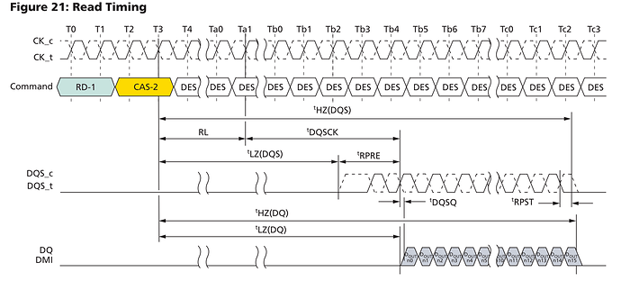
Figure 21: Read Timing
How determine cycle count for this example of read access?
T0->T3: RD-1, CAS-2, 3CK
T3->Ta1: RL=AL+CL (read latency = additive latency + CAS latency)
AL (additive latency, defined within MR (Mode Register) register:) 0, CL-1, CL-2
CAS latency (Column-Address-Strobe latency: cycles between internal READ command (and DQSCK latency) and availability of first bit of output data) for 1600MHz DDR4 : CL =~ 14-16 (prob. no half-clock latencies)
… RL =~ 14-31 (?) CK
Ta1->Tb4: 1-2CK
tLZ(DQS) - DQS Low Impedance Time from CK/CK#
tDQSCK (“is the actual position of a rising strobe edge relative to CK”, DDR4-3200 160ps =~ 1/4CK)
tDQSCK – DQS Output Access Time from CK/CK#
tDQSQ (skew between DQS and DQ)
tREFI (average interval of refresh commands (initiated by MC?) for device ~64ms/8192lines → (100us…) 7.8us (…0.9us) )
DQS_t (data strobe high pulse, true) DQS_c (data strobe low pulse, complement)
RPRE (Read Preamble, training/read leveling data strobe receivers, prog. to 1-2CK cycles, Tb2->Tb4)
RPST (Read Postamble)
Tb4->Tc2: 8 CK (data transfer time: ~5ns)
T0->Tc2: ~26-44CK (1600MHz: 16-27ns, 37-62.5MT/s*16bit*16(single ended traces) ~1.2-2GB/s each MC channel)
Tc2-> : precharge following to burst READ (BC4, BL8) ~4CK
READ (16bit data): ~(26-44)+4CK = ~(1-1.6)GB/s 1channel with precharge
consecutive READ (32bit data): ~(18-36)+16 =~(34-52)+4CK = ~(1.8-2.5)GB/s 1channel, incl. precharge
BC4 (64bit data): ~(18-36)+4x8=~(50-68)+4CK = ~(2.6-3.5)GB/s 1channel, incl. precharge
BL8 (128bit data): ~(18-36)+8x8=~(82-100)+4CK = ~(3.7-4.4)GB/s 1channel, incl precharge
[ BTW: another possibility might be hardware upgrade?
DDR5 Maintains Bandwidth with Increased Core Count, page 3
(non-linear increase of shared bandwidth with faster memory data frequency on multi core systems) ]

