Hi,
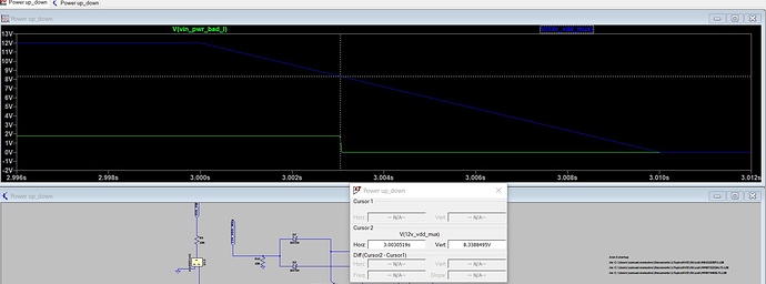
I am designing a custom carrier board for TX2. I have simulated the discharge circuit implemented on P2597 dev kit, and I have a doubt.
The discharge circuit works fine for the controlled case scenario (CARRIER_PWR_ON de-asserted after safe TX2 shutdown).
But when I simulate the uncontrolled case (removal of VDD_IN), I think the result is not as I expected, or I misunderstood the specifications. So in the case of VDD_IN removal, the discharge circuit needs to detect a voltage drop of approx. 20% of VDD_IN, and then assert VIN_PWR_BAD#, so the internal PMIC has time to perform a shutdown before VDD_IN drops completely (>2.9V).
I have noticed that is controlled by C49 on P2597 schematic. With 1uF value, in the picture attached it can be seen that VIN_PWR_BAD# is asserted when VDD_IN is already 0V, so the internal PMIC would have time to perform safe shutdown??
When I decrease the value of C49 to 100nF, the assertion happens at approx. 20% voltage drop.
Is 1uF the correct value of C49? Am I understanding correctly the power down performance?
Thank you.

