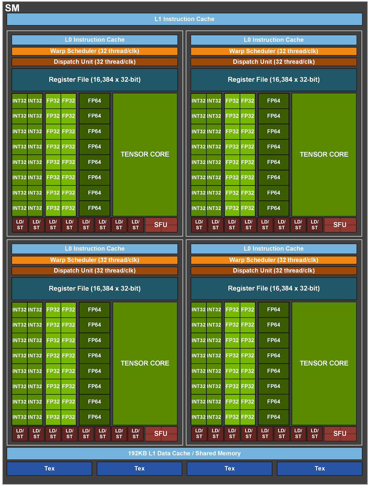
None of the boxes are memories except the register file (and the instruction cache in some way).
The INT32 units do integer calculations, the FP32 and FP64 units floating-point calculations. LD/ST are load-store units, the SFU calculates special functions (e.g. sin/cos).
As @rs277 already explained, when people speak of a GPU with n “CUDA cores” they mean a GPU with n FP32 cores, each of which can perform one single-precision fused multiply-add operation (FMA) per cycle. The number of “CUDA cores” does not indicate anything in particular about the number of 32-bit integer ALUs, or FP64 cores, or multi-function units, or “Tensor cores” (which I would also consider a marketing term).
If you want to know the throughput for various classes of operations, consult the CUDA Programming Guide rather than nice-looking block diagrams put out by the (technical) marketing guys.
Yes, but in isolation that does not mean very much. The number of each of these units dictates, (speaking broadly), how fast the SM can process a given instruction.
So if you wish to add INT32’s, each SM can process 4 x 16 = 64 per processor cycle. With only half the number of FP64 cores, this throughput halves to only 32.
Table 3 gives this information across the different GPU generations.