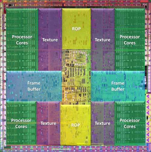
First, I’d like to clear up some confusion. There are basically two graphics explaining the GT200 die that circulate the web. [1, 2]
I assume the first one is correct: the blue block is a memory controller (comm logic) and not the frame buffer memory, correct?
Also, the “Texture” block makes me wonder… Are these texture processing units, or texture cache or both?
Finally, are there any more precise diagrams than these? Did Nvidia release any?
