Hello support,
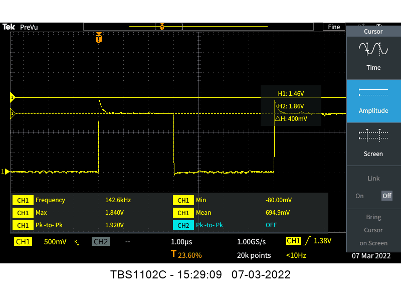
We are using our carrier board having Jetson Nano. We have level translator NTS0101PW to interface SPI devices at 3.3V. However, we found SPI MOSI & MISO signal levels settle to ~1.5V from 1.8V at rising edges of data. Please find attached waveforms. No such behavior in clock/ CS signal.
We are using 2 SPI, SPI0 & SPI, in both MOSI/ MISO settle to ~1.5V. To troubleshoot we lifted MISO of translator pin on 1.8V (Jetson side) & found signal was 1.8V on lifted pin. So issue appears after connecting to Jetson pins. Not sure why such behavior from Jetson side.
Apart from this, similar level translator is used in I2C & UART but voltage levels in other peripherals seems to be OK. Please advise ahead.
Regards,SPI0.rar (28.4 KB)SPI1.rar (29.2 KB)
Hi, can you see same behavior on your devkit? There are level shift on devkit too, if can’t be repro on devkit, then it looks more like the level shift issue.
Hi, there are other low & high frequency signals, UART, I2C which don’t show this issue & all using same level translator. It is only SPI MOSI & MISO signals (not even CLK & CS). Do you still think issue lies with level translator?
@jagdish.karamchandani
Hello,
What’s the REG by below command.
sudo cat /sys/kernel/debug/tegra_pinctrl_reg | grep -i spi
Hello,
Please find attached response to the said command.NVIDIA response.docx (11.7 KB)
Looks like the REG without problem.
sudo cat /sys/kernel/debug/tegra_gpio
sudo cat /sys/kernel/debug/tegra_pinctrl_reg | grep -i spi
Bank: 1 Reg: 0x70003050 Val: 0x0000e044 -> spi1_mosi_pc0
Bank: 1 Reg: 0x70003054 Val: 0x0000e044 -> spi1_miso_pc1
Bank: 1 Reg: 0x70003058 Val: 0x0000e044 -> spi1_sck_pc2
Bank: 1 Reg: 0x7000305c Val: 0x0000e048 -> spi1_cs0_pc3
Bank: 1 Reg: 0x70003060 Val: 0x0000e048 -> spi1_cs1_pc4
Bank: 1 Reg: 0x70003064 Val: 0x00006044 -> spi2_mosi_pb4
Bank: 1 Reg: 0x70003068 Val: 0x00006044 -> spi2_miso_pb5
Bank: 1 Reg: 0x7000306c Val: 0x00006044 -> spi2_sck_pb6
Bank: 1 Reg: 0x70003070 Val: 0x00006044 -> spi2_cs0_pb7
Bank: 1 Reg: 0x70003074 Val: 0x00006044 -> spi2_cs1_pdd0
Bank: 1 Reg: 0x70003078 Val: 0x0000e015 -> spi4_mosi_pc7
Bank: 1 Reg: 0x7000307c Val: 0x0000e015 -> spi4_miso_pd0
Bank: 1 Reg: 0x70003080 Val: 0x0000e015 -> spi4_sck_pc5
Bank: 1 Reg: 0x70003084 Val: 0x0000e015 -> spi4_cs0_pc6
Hello,
SPI0 _MISO.bmp (1.8 MB)
Did you configure the pin by jetson-io for devkit? Any device tree modification?
Could you use jetson-io to configure those pin with original system image without modification to check if device tree configure cause the problem.
Thanks
jagdish.karamchandani:
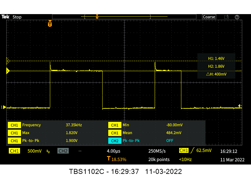
We took waveforms in Jetson Nano eval kit on 1.8V side for SPI0_MISO & results are same as our carrier board, i.e MISO line dips to 1.5V after peaking to 1.8V. However, there is no such behavior in clock/ CS signal of eval board which again is similar to our carrier board. Waveform attached.
Hello,
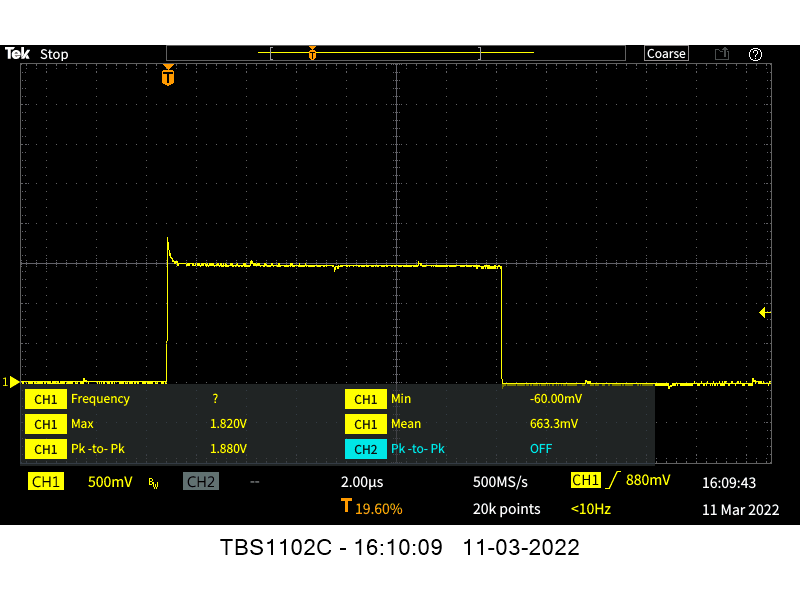
We see no change after using original system image & using Jetson-IO to configure, i.e we see distortion. Please see attached image for more clarity. Kindly advise further.
SPI0 _ MISO_11 Mar 22 (3).bmp (1.8 MB)SPI0 _ MISO_11 Mar 22 (2).bmp (1.8 MB)
Could you dump the REG and GPIO pin to check.
sudo cat /sys/kernel/debug/tegra_gpio
sudo cat /sys/kernel/debug/tegra_pinctrl_reg | grep -i spi
Bank: 1 Reg: 0x70003050 Val: 0x0000e044 -> spi1_mosi_pc0
Bank: 1 Reg: 0x70003054 Val: 0x0000e044 -> spi1_miso_pc1
Bank: 1 Reg: 0x70003058 Val: 0x0000e044 -> spi1_sck_pc2
Bank: 1 Reg: 0x7000305c Val: 0x0000e048 -> spi1_cs0_pc3
Bank: 1 Reg: 0x70003060 Val: 0x0000e048 -> spi1_cs1_pc4
Bank: 1 Reg: 0x70003064 Val: 0x00006044 -> spi2_mosi_pb4
Bank: 1 Reg: 0x70003068 Val: 0x00006044 -> spi2_miso_pb5
Bank: 1 Reg: 0x7000306c Val: 0x00006044 -> spi2_sck_pb6
Bank: 1 Reg: 0x70003070 Val: 0x00006044 -> spi2_cs0_pb7
Bank: 1 Reg: 0x70003074 Val: 0x00006044 -> spi2_cs1_pdd0
Bank: 1 Reg: 0x70003078 Val: 0x0000e015 -> spi4_mosi_pc7
Bank: 1 Reg: 0x7000307c Val: 0x0000e015 -> spi4_miso_pd0
Bank: 1 Reg: 0x70003080 Val: 0x0000e015 -> spi4_sck_pc5
Bank: 1 Reg: 0x70003084 Val: 0x0000e015 -> spi4_cs0_pc6
Below response for the command you suggested,
cat /sys/kernel/debug/tegra_gpio
Name:Bank:Port CNF OE OUT IN INT_STA INT_ENB INT_LVL
The configure without problem.
https://forums.developer.nvidia.com/t/155310/2
Shane–Could you let us know on what you are doubting, do you intend to change the slave device? Do you have source/ sink current capacities of IO in your mind creating issues? I will try loop back but can we try replacing slave device if it looks comfortable to you?
Current I only able to verify the SPI functionality by loopback test.
Also what do you mean replacing slave devices?
I mean hooking different SPI device instead of one that we are using now. We can take out SPI bus & connect to some different SPI slave device.