It seems you configured the wrong GPIO controller for sync-out-gpios.
Please use the following configuration instead. (i.e. use &gpio_aon instead of &gpio)
Thank you very much for your suggestions — I have successfully made the modification.
However, I noticed in the pinmux spreadsheet that the pin is set as input by default, but I need it to be output.
So I modified the pinmux spreadsheet and generated three .dtsi files.
I’m still using the AGX Orin platform. Could you please tell me which files in the official package I should replace with these three files to make my configuration take effect?
Please configure it as Output/Drive 0 in pinmux spreadsheet.
I would suggest checking the flash log to identify the exact file used for pinmux in your case. (pinmux_config)
Please put pinmux dtsi to <Linux_for_Tegra>/bootloader/generic/BCT and gpio dtsi to <Linux_for_Tegra>/bootloader/.
You may check the board config(p3701.conf.common) to know what is specified for PINMUX_CONFIG .
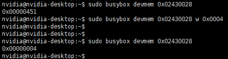
Okay, I have successfully verified it. I’m currently testing the use of the busybox tool to configure the GPIO direction (input/output). I found the offset address for GPIO3_PCC.02.
Pinmux register is used to configure the pin’s capability and use case rather than control high/low.
GPIO default state should be configured in gpio dtsi.
Please simply run the following command to check if it could be controlled.
I think you may have misunderstood my point. I used the official flashing package to update the system, and now I’m trying to change the GPIO direction (input/output) by directly modifying registers. However, it seems that writing to the registers doesn’t take effect — that’s the actual issue I’m facing. I would appreciate your help in figuring out why modifying registers using busybox is not working. Thank you!
This is the verification process I followed, so I suspect that the register configuration did not take effect.If there’s anything wrong with my verification approach, please kindly point it out. Thank you!