Hi all
I started to design the carrier for the orin nano before the dev kit was released this week so i had to use the Jetson Nano + Migration document to design it.
In the latest Jetson Orin Nano reference design (P3768_A04_Concept_schematics) you changed the power on/off circuit to use a EFM8SB10F2G chip…
I have used the reference from the Jetson nano as per my screenshot… I feel this is adequate and will suffice.
Do you feel my existing design is ok to use?
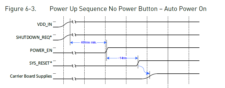
Hi, it looks fine. The key point is that your design should follow the power on sequence in Design Guide as below. You can check that on your nano board first.
Hi Trumany
Thanks for the reply, yes my power up sequence is as above. The 3.3V and 1.8V rails on the carrier are enables by SYS_RESET.
One question, I only have 1 power unput (regulated 5V) which immediately applies power to Vin of the Orin Nano…
In the Jetson nano reference, i am not sure when the VDD_5V_USB rail is powered if you only have a DC_JACK connected? How do the USB ports (VDD_5V_USB) get power if only the DC Jack is connected in the P3449_B01_Concept_schematics ?
I plan to power the VBUS pins of the USB2.0 connectors in my design with the VDD_IN (5V) rail.
Is this likely to be an issue? i.e powering VBUS at the same time as VDD_IN, before the SYS_RESET signal is high?
I think it will be ok, but wanted to check with you.
It depends on the USB port is host or device. If device, that’s OK to keep same as P3449. If host, you can refer to the USB1 port in Figure 6-1. USB Connection Example in Design Guide, a load switch is necessary.
ok, can you tell me when VDD_5V_USB become active on the P3449 schematic?
Is it as soon as DC input is applied?
There are two kinds of 5V supply to system on P3449, DC jack and USB VBUS. Your use case is similar to VBUS 5V supply only on P3449, so you can just use similar USB design of P3449 and short DC 5V to VBUS.
perfect, thanks for calrifying…
I was just overly concerned about powering the VBUS before module was ready.
Clearly its a non-issue and i will proceed by shorting DC 5V to VBUS!