Hi~
I’m HW engineer. We design a carrier board for Jetson Orin_NX/Nano module.
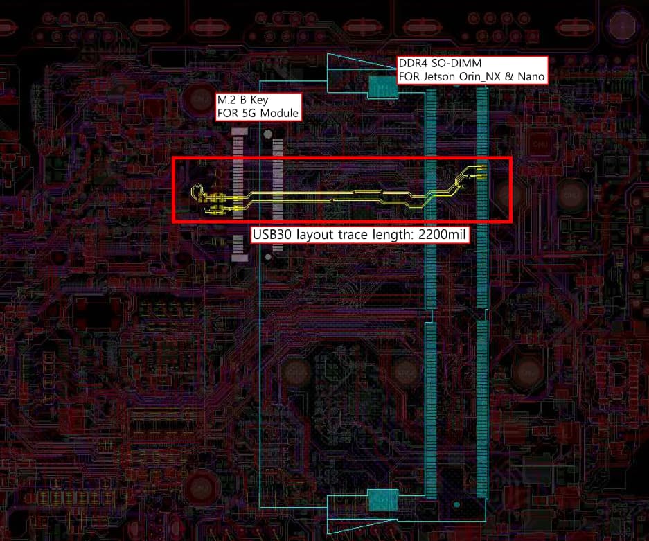
We measure the USB 3.2 Gen2 signal quality for both modules but only fail on Jetson Orin_Nano.
I think the layout design is not a problem. Does NV measure the USB 3.2 Gen2 signal quality for Jetson Orin_Nano?? What was the test result?
Hi, the USB part had been validated. And in fact, this part design in module is same between Orin NX and Orin Nano module. Can you share schematic of this part? And please check your layout design based on the USB 3.2 Routing Guidelines in Design Guide doc? There are some important items in the table that need you to check one by one.
Hi~
Could you tell me which version of the Jetson Orin Nano image does NV use to measure the USB 3.2 Gen2 signal??
I want to use the same image to measure the USB 3.2 Gen 2 signal for our board.
Also, I will double-confirm our USB 3.2 Gen 2 layout design.
Do you know which USB 3.2 routing guideline relates to the USB SSC test item?
Are you combining a USB2.0 port from a HUB with USBSS2? That’s not supported. Only below configuration is supported.
One USB2 roothub cannot be paired with multiple USB3 roothubs. Valid design is one USB2 roothub + one USB3 roothub like:
*) USB2 + USB3 in pair connecting to a USB HUB
*) USB2 + USB3 in pair connecting to a PD controller and then to a type-C port
*) USB2 + USB3 in pair connecting to a type-A port
Hi, We checked the item TSSC on Type C port of Orin Nano Developer Kit(Image:JP511-orin-nano-sd-card-image), and got the similar failed result.
I think it is not the schematic or layout problem. We have all USB3 items PASS, except TSSC. This item is to check spread spectrum.
The modulation rate of TSCC should be between 30.0 kHz to 33.0 kHz, but it reaches 160,170 kHz or more
is there any way to configure this value to fit USB 3.0 specification? orin_nx_nvidia_typeC.mht (320.5 KB)
Had you applied the patch of 0001-disabling-the-spread-Spectrum.patch? If had, it will disable SSC of USBSS too, as PLLE is shared between USB and PCIE. Once PLLE SSC is enabled/disabled, it affects both PCIE and USB. By default, PLLE SSC is enabled.
This will fix this in next release. For passing the compliance test for now, please put the device into SC7 first and resume. SSC will be enabled after this operation.