Hi NV Support Team
From document “Jetson_AGX_Orin_Design_Guide_DG-10653-001_v1.0”
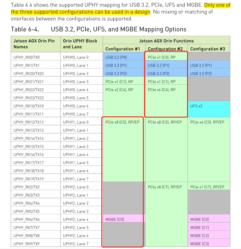
Table 6-4. USB 3.2, PCIe, UFS, and MGBE Mapping Options

-
PCIe x2 (C4), RP (as picture1 shown) is typo from Configuration #1? Actually, it should be PCIe x4 (C4) in configuration #1, right?
-
PCIe x4 (C5), RP/EP (as picture1 shown) is typo from Configuration #3? Actually, it should be PCIe x8 (C5) in configuration #3, right?
-
As Picture 2 shown, we use UPHY0 Block ( Lane 0 to Lane 7 ) as configuration #2, while UHPY1 Block(Lane 0 to Lane ) and UPHY2 Block(Lane0 to Lane7) as configuration #1, could this be OK?
-
Is Configuration #3 supported or could we use configuration #3 in our own design?