Hi,
I think there is a contradiction between the datasheet and the PDG.
In the datasheet:

Meaning, need to implement buffer on the carrier if used.
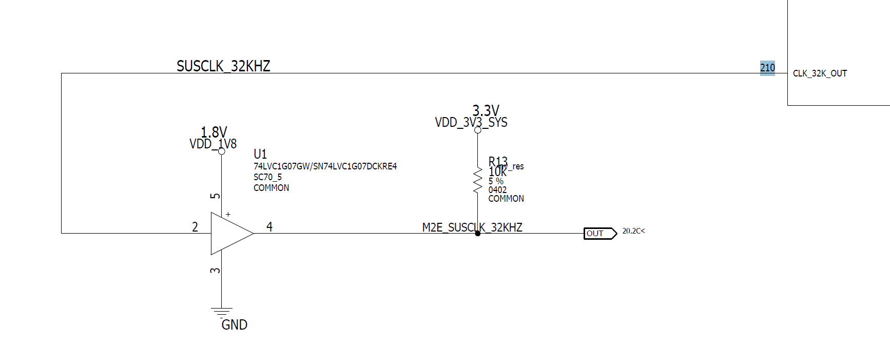
In the PDG:

Meaning, it is already buffered on the module.
Please advice.
Thanks,
Matan
Hi,
I think there is a contradiction between the datasheet and the PDG.
In the datasheet:
In the PDG:
Meaning, it is already buffered on the module.
Please advice.
Thanks,
Matan
Thanks you for your feedback. Product Design Guide is correct. The buffer on the module is to 1.8V level and refer to the carrier board design files, we do use a buffer to translate it to 3.3V levels on the carrier board.
Thank you for your answer,
This topic was automatically closed 14 days after the last reply. New replies are no longer allowed.