Hello, Andrey:
If you can develop your own carrier board, you can reserve UARTG pins for your own purpose.
br
Chenjian
Hello, Andrey:
If you can develop your own carrier board, you can reserve UARTG pins for your own purpose.
br
Chenjian
@jachen
is it correct that in order to implement SPE UART on AGX
it is required to change the defrault value
scr.2609.6 = 0x18002626; # AON_NOC_UARTG_BLF_CONTROL_REGISTER_0
to
scr.2609.6 = 0x18001616; # AON_NOC_UARTG_BLF_CONTROL_REGISTER_0
in the file
tegra194-mb1-bct-scr-cbb-mini.cfg
also change the file tegra19x-mb1-pinmux-p2888-0000-a04-p2822-0000-b01.cfg
to
pinmux.0x0c302048 = 0x00000401; # spi2_sck_pcc0: uartg,
pinmux.0x0c302050 = 0x00000459; # spi2_miso_pcc1: uartg,
Do we need to edit this file in the Jetpack folder?
/Linux_for_Tegra/bootloader/t186ref/BCT/tegra19x-mb1-pinmux-p2888-0000-a04-p2822-0000-b01.cfg
or
/Linux_for_Tegra/bootloader/tegra19x-mb1-pinmux-p2888-0000-a04-p2822-0000-b01.cfg
both? neither of the two?
also could we just flash dtb for UART SPE on AGX without reflashing OS?
Hello, Andrey:
Those information in SPE firmware doc only covers Xavier devkit.
For NX, some configuration files may be different.
An easy way is to check the flash log.
https://elinux.org/Jetson/L4T_BSP_development_tips#Edit_the_pinmux_configuration_file
search ’ Or check the flash log’.
Though that sample only shows PINMUX config file, other configs like SCR, etc., should be similar.
In flash, you can try -k to specify the partition name to be flashed. Kernel-DTB should be supported to do a single flash.
Note that not all partitions are supported by -k. A few partitions may contain information dependent on other partitions. You may meet ‘unsupported xxx’ if using -k to flash such parititons.
br
Chenjian
Hi Chenjian,
Thank you for your response.
I see how to flash dtb only, :
sudo ./flash.sh -k MB1_BCT jetson-xavier mmcblk0p1
but as part of config files that needs to be edited I am not sure if they will get applied if just to flash the dtb.
Could you also confirm that for AGX Xavier
t is required to change the defrault value
scr.2609.6 = 0x18002626; # AON_NOC_UARTG_BLF_CONTROL_REGISTER_0
to
scr.2609.6 = 0x18001616; # AON_NOC_UARTG_BLF_CONTROL_REGISTER_0
in the file
tegra194-mb1-bct-scr-cbb-mini.cfg ?
I will try with AGX Xavier at this time as NX UART SPE is not supported
@jachen
which of the three commands below will be correct for AGX?
sudo ./flash.sh -r -k DTB jetson-xavier mmcblk0p1
sudo ./flash.sh -k MB1_BCT jetson-xavier mmcblk0p1
sudo ./flash.sh -r -k kernel-dtb jetson-xavier mmcblk0p1Hello, Andrey:
For AGX Xavier, you can just follow the doc/uart.md steps.
br
Chenjian
@jachen Thank you for following up!
but as the doc/uart.md file has three points as listed below
In order to access a AON UART from the Cortex-R5 SPE/AON for Jetson AGX; the
UART SCR, and pinmux settings need to be updated as described in below steps.

1. Check SCR values as below in the file tegra194-mb1-bct-scr-cbb-mini.cfg:

       scr.2609.6 = 0x18001616; # AON_NOC_UARTG_BLF_CONTROL_REGISTER_0

2. Check default pinmux configuration as below in the file
   `tegra19x-mb1-pinmux-p2888-0000-a04-p2822-0000-b01.cfg`.

       pinmux.0x0c302048 = 0x00000401; # spi2_sck_pcc0: uartg,
       pinmux.0x0c302050 = 0x00000459; # spi2_miso_pcc1: uartg,

3. Compile device tree and flash the entire board to ensure that the SCR,
   and pinmux settings are flashed on the board.
will it require to run MB1_BCT to update the pinmux?
or just copy the dtp to Jetpack folder then flash it with kernel dtb?
could you provide the full flash.sh command that will include the two elements below or these wil be two separate flash.sh command? in which order they will need to be executed if so?
-k bootloader-dtb/_b and kernel-dtb/_b
What is the _b tail here? coud you extend, please?
I would just do one flashing command, but it will not be enough, right?>
sudo ./flash.sh -r -k kernel-dtb jetson-xavier mmcblk0p1
so after the command above should I also execute the command below?
sudo ./flash.sh -r -k bootloader-dtb jetson-xavier mmcblk0p1
like that?
in reverse order?
Hello, Andrey:
To test UART in SPE firmware, there are several components, like PINMUX, SCR, DTB, etc. to be updated.
The safe way is to flash the whole device fully with updated configurations/dtb. That may take a few minutes.
To save time, flashing specific partitions is also possible, as long as you know exactly what to do.
For this case, you can run command like:
sudo ./flash.sh -k MB1_BCT jetson-xavier mmcblk0p1
to update pinmux/SCR.
and
sudo ./flash.sh -r -k <part> jetson-xavier mmcblk0p1
to update kernel-dtb.
Since default SDK has A/B support, and bootloader DTB shares kernel DTB, part should be kernrel-dtb, kernel-dtb_b, bootloader-dtb, bootloader-dtb_b for a full update. Anyway, you can also just update kernel-dtb only if you are sure that partition is loaded.
br
Chenjian
while the first flas.sh worked kind of
sudo ./flash.sh -k MB1_BCT jetson-xavier mmcblk0p1
*** The [MB1_BCT] has been updated successfully. ***
the second kind of executed, but with warning
sudo ./flash.sh -r -k jetson-xavier mmcblk0p1
*** Update [jetson-xavier] is not supported. ***
The third one also seems worked
sudo ./flash.sh -r -k kernel-dtb jetson-xavier mmcblk0p1
*** The [kernel-dtb] has been updated successfully. ***
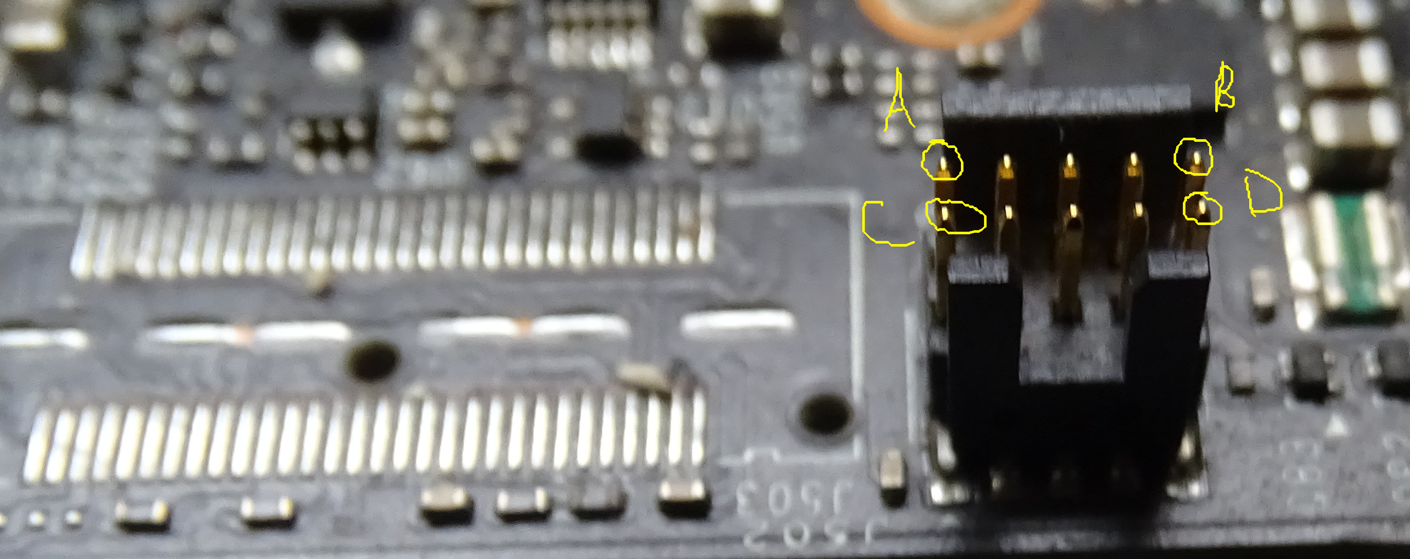
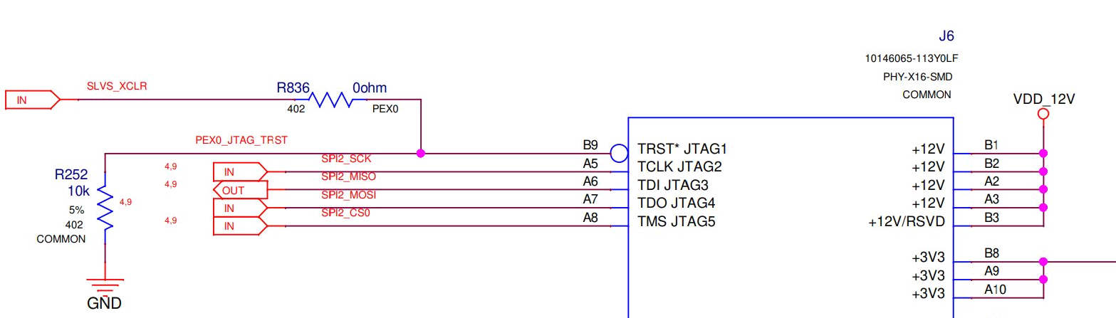
upd. I found J6 is PCI express x16 port, but which of it are the A5/ A6 pins?
Sorry, format typo, and it hides the actual characters.
Corrected.
As to pin, you can download the carrier board schematic and check with hardware engineer.
br
Chenjian
@jachen
could you confirm if we can access/ shortcut A5,A6 pins via JTAG pinouts?
from Design Schematics it appears that
A5 can be accessed through TCLK JTAG2
A6 can be accessed through TDI JTAG3
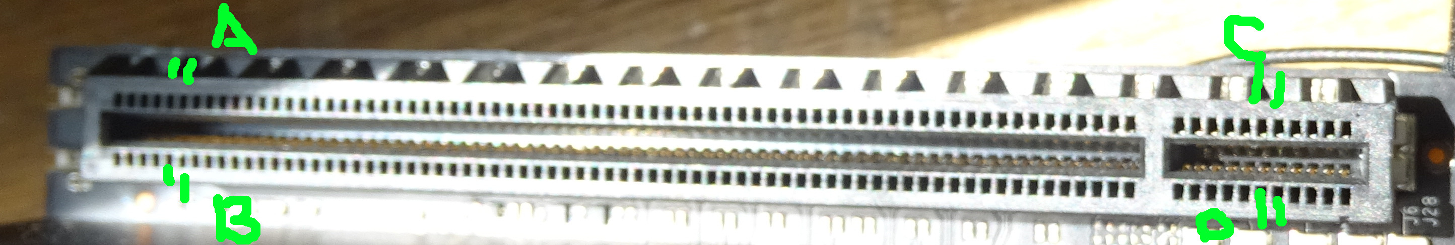
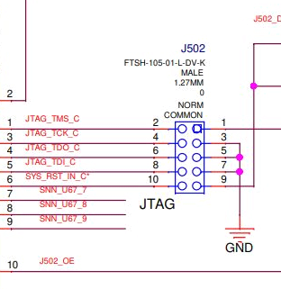
@jachen could you clarify, which of A,B,C,D is the pin1 so it would be possible to figure out which are the 2,3 pins to connet, please?
Hello, Andrey:
(Jetson AGX only)
UARTG TX/RX pins are in J6, A5/A6 which are in PCIe x16 slot. They have nothing to do with pins in J502. Please search SPI2_SCK and SPI2_MISO in carrier board schematic.
br
Chenjian
@jachen , Thank you for following up!
(Jetson AGX only)
yes, but you can see from the schematic excerpt attached that J6 header A5 is also labeled TCLK JTAAG2—SPI2_SCK
while J6A6 is labeled JTAG3 TDI—SPI2_MISO
Hello, Andrey:
You can download the carrier board schematic from Jetson download center.
A5/6 should be near ‘D’ as you marked.
In Jetson_Xavier_Developer_Kit_Carrier_Board_Design_Files_B03, P2822_B03_PCB_assembly_drawing.pdf, that’s near C142.
br
ChenJian