Hi Sir,
As title, what is the difference between UPHY lane & Serdes lane ?
Is a UPHY lane originated from a PCIe bus ?
What’s the logic behind it to distribute the UPHY lanes to high speed interface like PCIe, USB, UFS, M.2…and so on ?
How to config ODMDATA for that?
I know that my question might be basic. but could you provide more information ?
Thanks.
Jimmy
UPHY supports multiple interfaces like PCIe, USB3, MGBE. UPHY lane assignment/configuration needs to be one of the supported configurations in the design guide. ODMDATA allows to choose between supported UPHY lane configurations. Jetson AGX Orin Platform Adaptation and Bring-Up — NVIDIA Jetson Linux Developer Guide
@sgursal
Thanks for the reply.
Three more questions:
-
According to the block diagram of CVB p3737, specific UPHY lane are assigned to USB ports, as circled by red line as below:
My question is : how to assign a UPHY lane to a specific USB port ? Or there is a mapping table, for the 4 USB 3.2 ports & 4 USB 2.0 ports ?
-
How to map UPHY Lane 0 ~ UPHY Lane 23 to UPHY00~UPHY07, UPHY10~UPHY17 & UPHY20~UPHY27 ?
-
PCIe x 16 slot is used with 8 UPHY lanes, as below:

Why ? How about the missing upper x8, for x16 ?
Thanks.
Jimmy
@sgursal
Thanks for the prompt reply.
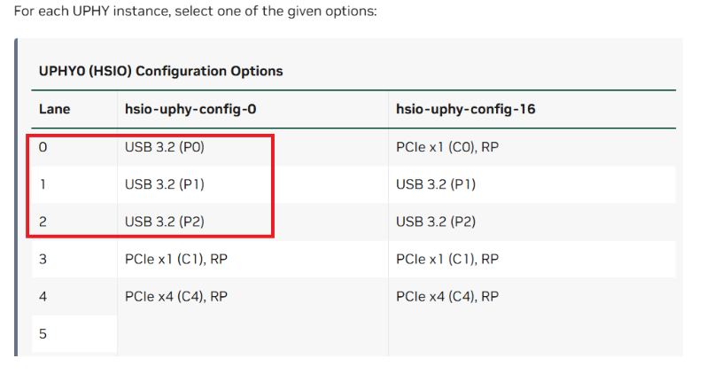
1. Please check the diagram & table below:
By the document you refer to, where is USB3 assigned with UPHY20 ?
- Following 1), P1 or P2 might be the USB port (3.2) for flashing. But inside the dtb, as below:
flashing port seems to be usb 2.0.
It is confusing.
- And I see no information about how to map UPHY Lane 0 ~ UPHY Lane 23 to UPHY00~UPHY07, UPHY10~UPHY17 & UPHY20~UPHY27 @ that document.
Please advise. Thanks.
Jimmy
Hi,
For the usb question I would suggest you could read the document first.
What I saw here is you just didn’t know how the device tree for USB part works
Flash port is a port supports both USB3 +USB2… so it would have usb2 lane + usb3 lane in use together.
Also, you actually should check table as below in the design guide. UPHY20 is USB3.2 P2.
@WayneWWW
Thanks for the prompt reply.
I will spend some time reading Adaptation_and_Bringup_for_Jetson_AGX_Orin
BTW, could you provide the link to the table "7.4 UPHY0 mapping options (USB & PCIE) ?
Since I can’t find it at
Welcome — NVIDIA Jetson Linux Developer Guide
Thanks.
Jimmy
Did you ever read the design guide before?
@WayneWWW
Hi Wayne,
I only read Linux developer guide, and I missed the design guide somehow.
Anyway, many thanks~
Jimmy
1 Like
@WayneWWW
One more question:
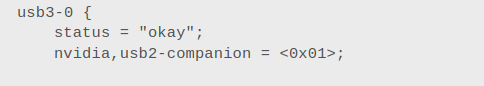
Please check the attached default dtb, as below:
and
So, the OTG port is usb2-0\usb3-0.
But , according to the attached below:
USB3-1 claims that its USB2 companion port is USB2-0.
Is there any conflict here ?
Thanks.
Jimmy
The phy-names in usb@3550000 are just a fixed string. It does not really link to any USB lane.
In brief, no matter what usb3 node you added there, this phy-names is always usb2-0/usb3-0.
Only the nvidia,usb2-companinon field represents the true link.
@WayneWWW
Hi Wayne,
Another question:
PCIe x 16 slot is used with 8 UPHY lanes, as below:
Why ? How about the missing upper x8, for x16 ?
Thanks.
Jimmy
Yes, only 8 lanes could be in use but that does not matter because the software would still support.
@WayneWWW
I still have some questions about USB DT:
- according to the diagram above, USB 0 goes with UPHY lane 1, while USB1 goes with UPHY lane 0.
But according to the development doc:
USB0 goes with UPHY lane 0, and USB1 goes with UPHY lane1, instead.
Isn’t it conflicted ?
-
I disassembled the default kernel DT as below:
ports {
 		usb2-0 {
 			status = "okay";
 			vbus-supply = <0xf9>;
 			mode = "otg";
 			usb-role-switch;

 			port {

 				endpoint {
 					remote-endpoint = <0xfa>;
 					phandle = <0x10f>;
 				};
 			};
 		};

 		usb2-1 {
 			status = "okay";
 			vbus-supply = <0xf9>;
 			mode = "host";

 			port {

 				endpoint {
 					remote-endpoint = <0xfb>;
 					phandle = <0x10d>;
 				};
 			};
 		};

 		usb2-2 {
 			status = "okay";
 			vbus-supply = <0xf9>;
 			mode = "host";
 		};

 		usb2-3 {
 			status = "okay";
 			vbus-supply = <0xf9>;
 			mode = "host";
 		};

 		usb3-0 {
 			status = "okay";
 			nvidia,usb2-companion = <0x01>;

 			port {

 				endpoint {
 					remote-endpoint = <0xfc>;
 					phandle = <0x10e>;
 				};
 			};
 		};

 		usb3-1 {
 			status = "okay";
 			nvidia,usb2-companion = <0x00>;

 			port {

 				endpoint {
 					remote-endpoint = <0xfd>;
 					phandle = <0x110>;
 				};
 			};
 		};

 		usb3-2 {
 			status = "okay";
 			nvidia,usb2-companion = <0x03>;
 		};

 		usb3-3 {
 			status = "disabled";
 		};
 	};
I thought the numbering of USB ports are as below,
USB 0: usb2-0, usb3-0
USB 1: usb2-1, usb3-1
USB 2: usb2-2, usb3-2
USB 3: usb2-3, usb3-3
According to the block diagram of the P3737 carrier board, USB 2(going through M.2 Key E socket) is the only port that doesn’t support USB 3.2 . But according to DT listed above, the port should be USB 3, since its usb3-3 is disabled.
In other words, I am confused about the numbering of USB ports here.
Please advise. Thanks.
Jimmy
Because your understanding to the device tree is incorrect…
The document is all correct.
This means USB3-0 (P0) is with usb2-1.
Your understanding to this picture is also incorrect.
“P0” in this picture means USB3-0 in the device tree.
“P1” menas USB3-1.
It has nothing to do with what USB2 connected to. I mean this table does not indicate anything for USB2.
@WayneWWW
Thanks for the prompt reply.
By the table above, does it also mean that USB3-2 in the device tree must use UPHY lane 2 ?
However, the block diagram below indicates that USB3-2 (using hub) goes with UPHY lane 20.
Thanks.
Jimmy
The problem here is you keep got misled by the Pin names of AGX Orin module and the SoC.
The mapping of usb3.2 (P0-P2) is a fixed thing. They are on the fixed UPHY.
You could read this table to understand this more clearly. Please make sure you don’t get confused by UPHY0 lane0-7 of the SoC and UPHY lane 0-20 of the AGX module
For example, USB3.2 P0 is usb3-0 in the device tree. For Soc, it is UPHY0 lane 0 and for module, it is UPHY0. And USB3.2 P1 is usb3-1, UPHY0 lane1 and UPHY1 for module.
@WayneWWW
Many thanks!
And I am trying to modify DT to fit our carrier board, and according to the default config:
		ports {
			usb2-0 {
				mode = "otg";
				usb-role-switch;
				status = "okay";
				port {
					hs_typec_p1: endpoint {
						remote-endpoint = <&hs_ucsi_ccg_p1>;
					};
				};
			};

			usb2-1 {
				mode = "host";
				status = "okay";
				port {
					hs_typec_p0: endpoint {
						remote-endpoint = <&hs_ucsi_ccg_p0>;
					};
				};
			};

			usb2-2 {
				mode = "host";
				status = "okay";
			};

			usb2-3 {
				mode = "host";
				status = "okay";
			};

			usb3-0 {
				nvidia,usb2-companion = <1>;
				status = "okay";
				port {
					ss_typec_p0: endpoint {
						remote-endpoint = <&ss_ucsi_ccg_p0>;
					};
				};
			};

			usb3-1 {
				nvidia,usb2-companion = <0>;
				status = "okay";
				port {
					ss_typec_p1: endpoint {
						remote-endpoint = <&ss_ucsi_ccg_p1>;
					};
				};
			};

			usb3-2 {
				nvidia,usb2-companion = <3>;
				status = "okay";
			};
		};
	};
Could you tell me , what is the difference between
hs_typec_p1
hs_typec_p0
ss_typec_p0
ss_typec_p1
?
I guess that the prefix “hs” might refer to high speed for USB 2.0, and “ss” might refer to super speed" for USB 3.2. But suffix “p0” or “p1” seems not to go with usb2-0, usb3-0, usb2-1 or usb3-1.
Please advise. Thanks.
Jimmy