Hello,
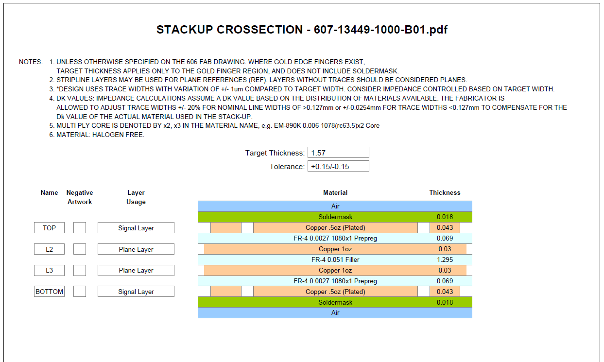
I’m looking into design a carrier board for the Jetson Nano and I’m setting up my board stack up and impedance controlled trace dimensions. I wanted to replicate the dimensions of the development board as close as possible, however when I input the trace dimensions into online impedance calculators the differential impedance it outputs doesn’t match the impedance given in the P3449_B01_PCB_stackup document. Perhaps I have made an error with units or dimensions, so it would be good to understand why the calculations don’t match. I believe all units are in mm as stated at the bottom of the document.
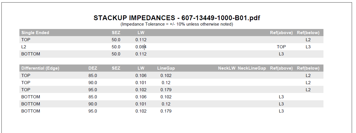
Below I have input the the 85ohm edge coupled differential impedance trace dimensions into the calculator provided by EEWeb.
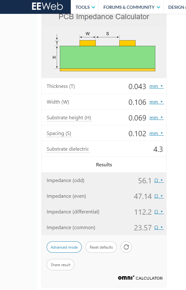
I notice that the single ended 50ohm trace dimensions do give ~50ohms impedance when input into the calculator.
I have tried different differential edge coupling calculators and get similar results which don’t match the stack up documentation. I’ve tried varying the copper thickness to account for differences in how plating is accounted for and varying Er within reason but can’t get the values close.
Any thoughts on the discrepancy would be appreciated. I’d like to understand where the error is before proceeding and including it in my design.