两块agx orin开发板用pcie交叉线连在一起,一块做rc端,一块做ep端,并按照PCIe Endpoint Mode — NVIDIA Jetson Linux Developer Guide 1 documentation 烧录了固件并做了ep端配置。现在在rc端用lspci命令检测不到ep端的板子。
系统版本:Jetpack6.2 [L4T 36.4.3],产品型号:900-13701-0050-000,RC端、EP端dmesg日志如下:
请问是什么原因呢?
rc.log (59.5 KB)
ep.log (61.3 KB)
Hi cdliyijie,
Could you share the block diagram how do you connect 2 AGX Orin devkit through PCIe interface?
Please also share the device tree configurations for both rc and ep sides.

It seems these 2 dts are exact the same.
Please check if you’ve provided the correct dts file for both rc and ep sides.
是的,rc端和ep端的设备树文件是一样的,我确认了。
线序图如下:
反序PCIE线的PIN连接关系_20250604_20250604151820.pdf (2.0 MB)
I would expect that the configuration for EP side should be different.
Hi
Please share your latest EP and RP side log. I saw you had some new update but never gave out new log anymore.
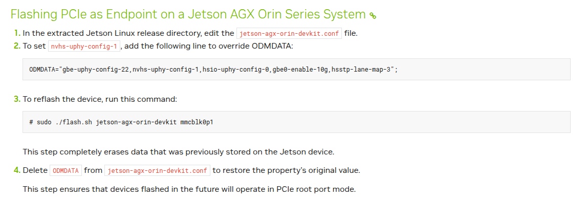
两块板子的硬件组成完全相同,只是在烧写之前将配置文件改成了对应的RP和EP端配置,这种情况下,RP和EP端设备树文件应该相同还是不同呢?
The question here is what kind of “烧写之前将配置文件改成了对应的RP和EP端配置” did you try there..
If you modified the ODMDATA, then our overlay dtbo will handle the device tree content automatically. But if you didn’t apply our overlay dtbo, then such change won’t happen.
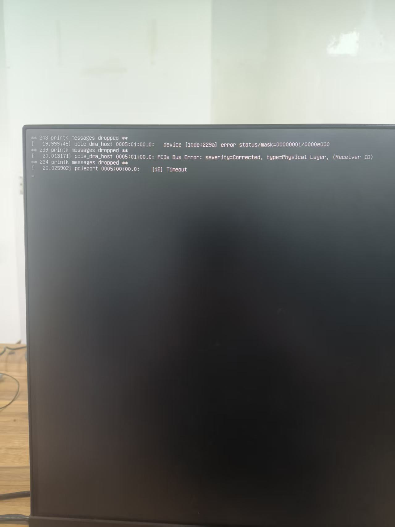
这是最新的ep端日志:
ep.log.txt (60.6 KB)
rp端由于引导阶段报错,无法查看日志
Learn to dump from uart.
there is no such “ rp端由于引导阶段报错,无法查看日志”. It only means you didn’t dump the log from uart.
最新的rp日志:
rp.log.txt (393.5 KB)
please refer to the hardware design.
Even though it is Xavier doc, it is still applicable to Orin.
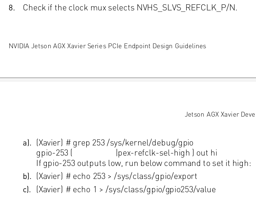
Those are not needed for Orin.
我们对硬件设计做了检查,以下是我们的排查记录,是否有漏掉或做错的地方?
AGX硬件验证记录-20250613.doc (527.5 KB)
下一步我们应该怎么做,是否能给我们一些建议?
Please write things in English first. Some engineers here do not read Chinese.