Hi,
We have designed a custom carrier board. Now there are 2 problems.
1: I use this carrier board to flash AGX Xavier, but it pauses and cannot continue. Here is the printed information,see the picture.
2: Then, I replace another AGX Xavier that has been flashed . After I press the power button, the power on sequence meets the requirements, see the pictures. But the system did not start.
In addition to the power on sequence, are there any other factors that will affect the startup ?
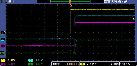
The Oscilloscope has 4 channels, so I upload 3pictures to show the whole power on sequence.
channel 1: BUTTON_POWER_ON*
channel 2: POWER_BTN_N
channel 3: VIN_PWR_ON
channel 4: SYS_VIN_HV (12V)
BUTTON_POWER_ON is pulled up to 3V3_AO(always on) , so once I insert the DC jack, BUTTON_POWER_ON is drived high.
POWER_BTN_N is pulled up to VDD_3V3, so after I insert the DC jack,there is no voltage,until the MCU drive it or after CARRIER_POWER_ON assert.
So,these pictures can prove that theMCU is working and the AGX Xavier module also asserts CARRIER_POWER_ON.
Are VDD_3V3 and VDD_1V8 the all power rails of carrier? Is there other power rail? If no other rail, and all power rails are ON correctly after module, then you can compare your design to reference to see how many different points between them and try to find out if it is the root cause. From HW side, it is hard to tell what cause that, maybe you can start from the check list sheet attached in Design Guide. That sheet lists many important items which need to be carefully handled.