Hi NV Support Team
We want to used ORIN & MAX96712 for C PHY design.
We follow up From DG-09364-001_v1.4.pdf. So we need update register for lane1 to 010=ABC to BCA
The swizzle registers should be set as follows for C PHY mapping.
• POLARITY_SWIZZLE_CPHY0_A (control for lane 0): 000 = ABC to ABC
• POLARITY_SWIZZLE_CPHY1_A (control for lane 1): 010 = ABC to BCA
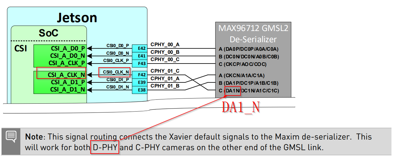
The Figrue 3-4 for ORIN&MAX96712 connection support both C-PHY and D-PHY ?
CPHY: Polarity for lane1 change to 010.
DPHY: CLK_N<=>CLKCN / D1_P<=>DA1P / D1_N<=>DA1N.
Some confuse for figure 3-3.
If we use DPHY the CSI_A_CLK_N connect to DA1_N. I dont think it is correct for DPHY use case. From MAX96712 datasheet if setting as DPHY, the DA1_N means Data 1_N not CLK_N.
Why you comment the guide is correct for D-PHY connection?
From MAX96712 datasheet the DA1N: D-PHY Port A data Lane1 inverted ouput.
But your guide connect to CSI_A_CLK_N. Can you please double check again.
Hi Trumany
I have double check your design guide.
Some conflict in document. e.g. the 3.3 show the mapping #2 in table 3-2 support both D-PHY and C-PHY.
The mapping same as figure 3-4
So from my understanding we can used figure 3-4 / mapping #2 to support both D-PHY and C-PHY.
Please help check with your RD, if the design guide wrong. Please also update design guide.
Hi,
We will update Jetson AGX Orin Series Camera Module Hardware Design Guide:
Figure 3-3 note: only CPHY is supported.
Figure 3-4 note: both CPHY and DPHY could be supported.
Please double check the de-serializer spec to confirm the connection.