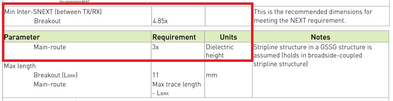
Q2: The “Min Inter-SNEXT” in the USB 3.0 Design Guidelines(Table 7-8. ) below is 4.85x (3x) for what dimension?
and, what does “dielectric height” mean?
Q1, it is a typo which should be mm not inch.
Q2, The unit is Dielectric height same as Main-route which is similar as you can see in “Max length” row. Dielectric height is the height of dielectric layer of PCB, you can find that of devkit carrier board in “stackup” file in the carrier board files package. http://developer.nvidia.com/embedded/dlc/jetson-xavier-developer-kit-carrier-board-design-files-b03